
 By
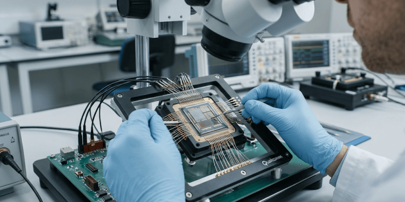
SAN DIEGO, United States — Qualcomm Technologies has completed hardware validation of its first-generation High Bandwidth Compute silicon, marking an important engineering milestone in its development of next-generation artificial intelligence infrastructure. Announced on November 2, 2026, the validation demonstrated the full memory read-write pathway and near-memory computing capabilities of the company’s architecture. Qualcomm intends to use the technology in future AI inference platforms, including its planned Dragonfly AI250 accelerator.
The development addresses one of the important challenges in large-scale AI computing: moving data efficiently between memory and processing components. As artificial intelligence models become more capable and are used by larger numbers of customers, the amount of data that must be accessed during inference continues to place pressure on computing systems.
High Bandwidth Compute Targets Memory Bottlenecks
AI inference requires processors to repeatedly access model information while generating outputs. Moving large volumes of data between memory and compute components can increase latency, energy consumption, and the overall cost of operating AI systems.
Qualcomm’s High Bandwidth Compute architecture is designed to address this challenge by placing computing capabilities closer to memory. The approach aims to reduce unnecessary data movement and improve the efficiency of workloads that depend heavily on memory bandwidth.
The company said its first-generation silicon successfully exercised the complete memory read-write path and near-memory computations using production-representative data pathways. These tests were conducted in Qualcomm’s San Diego laboratory using industry-standard automated test equipment.
Silicon Validation Marks an Engineering Milestone
Qualcomm described the results as evidence that the core technology is operating as designed. The validation moves the project beyond earlier architectural development and testing stages, providing a physical silicon implementation for further product integration.
The company also highlighted work involving advanced packaging, wafer bonding, defect management, and reliability. These engineering areas are important for technologies that integrate memory and logic more closely within a computing system. The ability to manufacture such designs consistently will be essential before they can be deployed commercially at scale.
Dragonfly AI250 Is the Next Development Stage
Qualcomm plans to integrate High Bandwidth Compute into its Dragonfly AI250 accelerator, which it expects to begin sampling in the first half of 2027. The product is intended for AI inference workloads and forms part of the company’s wider effort to develop data centre computing infrastructure.
The company said a data centre product has already taped out and that early bring-up work involving a logic base with bonded DRAM tiers is underway. These developments indicate progress toward product integration, although the commercial performance and availability of the eventual system remain to be demonstrated.
Energy Efficiency Becomes a Key AI Infrastructure Priority
The cost of running AI infrastructure increasingly depends on more than processor performance alone. Memory bandwidth, energy consumption, cooling, and data movement all contribute to the total cost of serving AI workloads.
Technologies that improve performance per watt could become valuable as cloud providers and enterprises expand their inference operations. However, real-world benefits will depend on final product implementation, workload characteristics, manufacturing yields, and system-level performance.
Qualcomm’s validation milestone represents progress toward its next-generation AI hardware strategy. The next major test will be whether the architecture can translate laboratory results into reliable, commercially deployable computing systems.














Comments